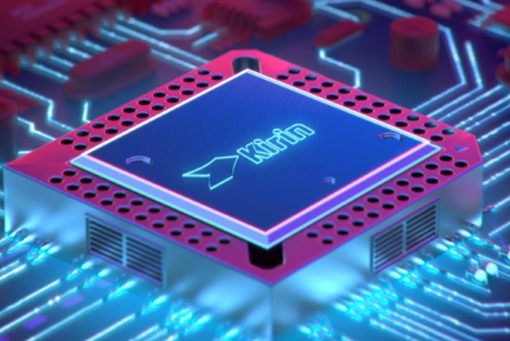
[CHIPS] [Progress] [芯片战役具体行动] 中国芯片发展 [2020-2030] ZGZL July 12, 2020 [CHIPS] [Progress] [芯片战役具体行动] 中国芯片发展 [2020-2030]2020-12-18T19:40:28+00:00 中国安全复兴关键指标 - List, 半导体芯片 (华为保卫战) 128 CMTS xlpharmacy viagra last reply @ December 25, 2024 中国芯片技术自主发展 2020 美国技术封锁华为光刻机芯片一直是中国进口金额最大的商品。根据海关公开数据,2019年中国芯片进口额为3040亿美元,超过原油、铁矿砂、粮食总和3016亿美元。美国限制芯片出口的行动,一定程度上激起了自主研发芯片的决心和力量。此次四部门联合发布支持集成电路发展的政策,将加快我国集成电路产业的发展。 Related Posts [Chips] Knowledge [Auto] [Car] JAC 中企进军 拉美 & 欧美汽车市场 [孟晚舟] 2018 华为首席财务官孟晚舟被捕 (加拿大-美国) [On-Going]
![[Chips] Knowledge](https://www.zgzl2050.com/wp-content/uploads/2020/12/image-19-200x120.png "[Chips] Knowledge")
![[Auto] [Car] JAC 中企进军 拉美 & 欧美汽车市场](https://www.zgzl2050.com/wp-content/uploads/2020/10/jac-200x120.jpg "[Auto] [Car] JAC 中企进军 拉美 & 欧美汽车市场")
![[孟晚舟] 2018 华为首席财务官孟晚舟被捕 (加拿大-美国) [On-Going]](https://www.zgzl2050.com/wp-content/uploads/2020/04/image-111-200x120.png "[孟晚舟] 2018 华为首席财务官孟晚舟被捕 (加拿大-美国) [On-Going]")
xlpharmacy viagra
xlpharmacy viagra
is cipro a sulfa drug
is cipro a sulfa drug
is keflex the same as cephalexin
is keflex the same as cephalexin
pregabalin schedule
pregabalin schedule
what class of drug is trazodone
what class of drug is trazodone
amoxicillin with clavulanate
amoxicillin with clavulanate
lisinopril erectile dysfunction
lisinopril erectile dysfunction
gabapentin for pain
gabapentin for pain
how long do side effects last after stopping tamoxifen
how long do side effects last after stopping tamoxifen
can i drink alcohol while taking valacyclovir
can i drink alcohol while taking valacyclovir
is doxycycline a very strong antibiotic?
is doxycycline a very strong antibiotic?
modafinilo que es
modafinilo que es
prednisone for gout
prednisone for gout
cephalexin 500mg cap
cephalexin 500mg cap
glucophage gluten
glucophage gluten
how long do side effects of augmentin last
how long do side effects of augmentin last
sildenafil vs tadalafil vs vardenafil
sildenafil vs tadalafil vs vardenafil
tadalafil works by blocking pde5 nitric oxide
tadalafil works by blocking pde5 nitric oxide
no prescription online viagra
no prescription online viagra
buy stromectol canada
buy stromectol canada
cost of ivermectin medicine
cost of ivermectin medicine
ivermectin 80 mg
ivermectin 80 mg
price of tadalafil
price of tadalafil
comprar vardenafil generico
comprar vardenafil generico
ivermectin 3mg
ivermectin 3mg
stromectol tablets uk
stromectol tablets uk
brand viagra online canadian pharmacy
brand viagra online canadian pharmacy
ivermectin 90 mg
ivermectin 90 mg
purchase levitra online
purchase levitra online
buy sildenafil online
buy sildenafil online
tadalafil price walmart
tadalafil price walmart
lidocaine cream pharmacy
lidocaine cream pharmacy
online pharmacy no prescription zithromax
online pharmacy no prescription zithromax
cialis online pills
cialis online pills
sildenafil for women
sildenafil for women
levitra 20mg buy
levitra 20mg buy
synthroid competitors
synthroid competitors
voltaren gel for
voltaren gel for
max dose of spironolactone for pcos
max dose of spironolactone for pcos
ivermectin cream canada cost
ivermectin cream canada cost
sitagliptin chf
sitagliptin chf
coming off venlafaxine
coming off venlafaxine
how long does it take for tizanidine to work
how long does it take for tizanidine to work
tamsulosin hydrochloride price
tamsulosin hydrochloride price
abilify and alcohol
abilify and alcohol
ramipril lactose
ramipril lactose
acarbose china
acarbose china
robaxin and aleve
robaxin and aleve
protonix 40 mg
protonix 40 mg
semaglutide tablets price
semaglutide tablets price